
EXPLORE. EXPERIMENT. ENGINEER.
Bulk Crystal Growth
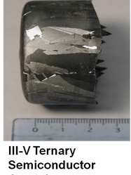
We specialize in bulk crystal growth of ternary and doped binary III-V semiconductor compounds. Depending on customer’s need, we can grow crystals with diameter in the range of 1 to 6 inches (25 – 150 mm). The cut-off wavelength (corresponding to the energy bandgap of the semiconductor) can be varied by changing the alloy composition. Our proprietary crystal growth method provides uniform chemical composition crystals along the length of boule as well as across the entire wafer surface. Our crystal growth conditions are fine tuned to provide uniform and the highest optical transmission through the wafers with lowest possible optical defect density. Dopant impurities are used in precise concentrations to compensate for the equilibrium native n-type and p-type defects present in the crystals, thereby enhancing the optical transmission of the wafers and obtaining the desired electrical resistivity of the substrates. Crystals grown by us are listed below:
-
Ga1-xInxAs (0 < x <1; cut-off wavelength: 0.87 – 3.5 micron)
-
Ga1-xInxSb (0 < x <1; cut-off wavelength: 1.7 – 7.0 micron)
-
Ga1-xInxP (0 < x <1; cut-off wavelength: 0.5 – 0.9 micron)
-
InAs1-yPy (0 < y <1; cut-off wavelength: 0.9 – 3.5 micron)
-
GaSb (doped with Te, Se, S, Zn, Cd)
-
InAs (doped with Te, Se, S, Zn, Cd)
-
InSb (doped with Te, Se, S, Zn, Cd)
If you are interested in semiconductor materials not listed above, we can develop the crystal growth process to grow the compounds of desirable chemical composition and impurity concentration. Contact us for discussing your crystal needs.
Research Samples
We have grown a variety of small size crystals for our customer’s fundamental research projects. Selected list of materials include: Ga1-xErxAs, Ga1-xErxSb, KNbO3, Ga2O3, In2O3, CdS, ZnS, CdSe, CdTe, ZnSe, ZnTe, TiO2, ZnO, Zn1-xCdxS, ZnS1-ySey ,ZnSe1-yTey, Zn1-xCdxO, Zn1-xCdxTe, Zn1-xCdxSe, GaSe, GaS, GaSeS, GaTe, AlGaSb, AlInSb, YAG:Ce, Rare-earth doped glasses (phosphors), SixGe1-x. If you are interested in any of these materials or related compounds, we can develop the crystal growth process to grow the compounds of desirable chemical composition and impurity concentration.
Contact us for discussing your sample needs.


Luminescent Powders
We have synthesized luminescent powders for a variety of applications. Selected class of materials include: Silicates, Garnets, Thiogallates, Oxides, Oxy-sulfides, Sulfides and Selenides. If you are interested in any of these materials or related compounds, we can develop the synthesis process to grow the compounds of desirable chemical composition and activator species.
Contact us for discussing your phosphor needs.
Nano-inks
We have prepared inks of high quality semiconductors nano-crystals dispersed in both organic solvents and water. Size range of nano-crystals can be tuned in the range of 10 nm to 500 nm. These inks have been used to deposit thin films of III-V semiconductors on substrates of ceramic, glass, metal and other semiconductor materials for fabricating devices such as solar cells, photodetectors and Terahertz generators. Selected list of nano-ink materials include: InP, GaAs, GaP, InAs, GaSb, InSb, GaInAs, GaInSb, InAsP, GaInP, ZnCdS, ZnCdTe, SiGe. If you are interested in any of these materials or related compounds, we can develop the ink of desirable chemical composition in desirable organic solvents or water.
Contact us for discussing your nano-ink needs.

Wafer Slicing & Dicing
We can help slice wafers from any boules or ingots with diameter up to 75 mm (3 inches). We have proprietary process for damage-free (avoiding fracture) slicing of fragile materials. We provide slicing and dicing services for customer specific materials. A variety of mechanically unstable materials such as nonlinear optic glasses (such as As-Se), GaSe, II-VI semiconductors, organic crystals, as well as mechanically very hard crystals such as SiC, Sapphire, Silicon, have been sliced by our process with minimal fracture and edge losses. After wafer slicing, we also help in dicing wafers into smaller size with specific dimensions as per our customers need. We also fabricate optical components of different shapes like prism, polygon, cubes, etc.
Contact us for discussing your slicing and dicing needs.


Wafer Grinding & Polishing
We have wafer grinding (to reduce thickness) and chemical-mechanical polishing facilities. We provide high quality surfaces that are necessary for optical and electrical characterization of materials. Our proprietary grinding and polishing process minimizes wafer chipping and fracture during processing. We have successfully processed a large variety of mechanically soft and hard materials. We can handle wafers up to 75 mm (3 inch) diameter with any shape. We also provide polishing of optical components like prism, polygon and cubes, etc.
Contact us for discussing your grinding and polishing needs.

Impurity Diffusion, Activation & Annealing
We provide high temperature diffusion, activation and annealing processes. Impurity diffusion and annealing are necessary for making p-n junction devices, healing defects in crystals and wafers, activating color centers in luminescent materials, improving mechanical and crystal quality, etc. We have the facility (furnaces and chambers) to conduct these processes up to a temperature of 1800 oC under various ambient (vacuum, inert gas like nitrogen, argon, hydrogen, or mixture of these gases, oxygen) either as rapid thermal annealing or an extended duration process.
Contact us for discussing your impurity diffusion, activation
and annealing needs.

Wet Chemical Etching, Cleaning & Passivation
We provide wet chemical etching and cleaning services for a large range of materials. We have comprehensive set of processes for selective etching of various semiconductors, oxides and metals. We also develop new recipes for etching and chemical cleaning process for our customers based on their materials composition and device structures. We can provide epi-ready surface processing and surface passivation services.
Contact us for discussing your wet chemical etching, cleaning and surface passivation needs.


